A discrete-circuit BJT amplifier is a board-level BJT amplifier: individual transistor and resistors, biased from a single supply, with capacitors that separate the DC bias from the AC signal. The standard form is the four-resistor common-emitter stage.
Four-resistor voltage-divider bias
The biasing scheme is the Voltage-divider bias four-resistor topology:
- (from to base) and (from base to ground) form a divider that pins the base voltage .
- from collector to .
- from emitter to ground.
Then and set the operating point, independent of , provided the divider current is much larger than the base current (rule of thumb, 5–10×). If the divider were starved, would load it and a -dependent error would creep back in; sizing it stiff is what holds the bias steady. The DC procedure is BJT DC analysis; the other common bias schemes (single-resistor, divider+, dual-supply, collector-to-base feedback) are summarised below.
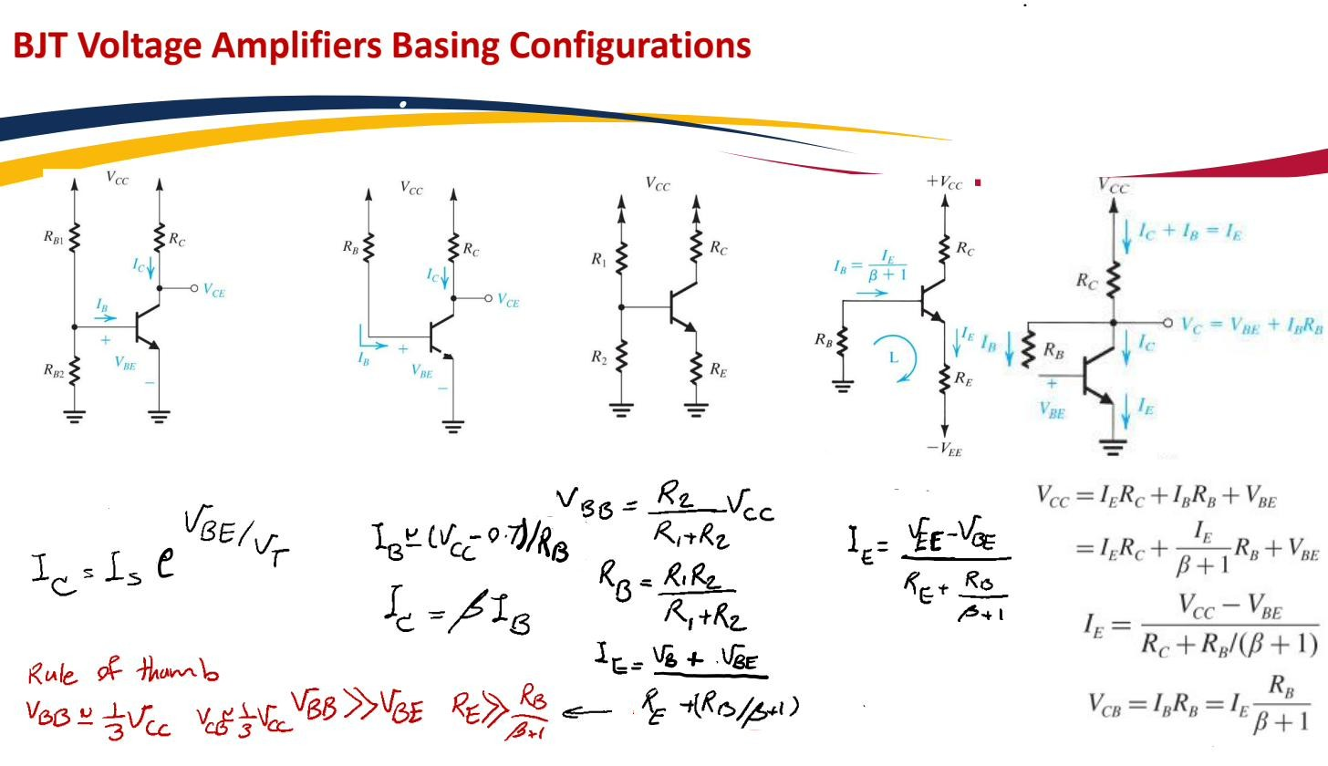 BJT bias schemes left to right: four-resistor voltage divider, single-resistor, voltage-divider with emitter resistor, dual-supply , and collector-to-base feedback. The slide title “Basing” is a typo for “Biasing.” The voltage-divider and dual-supply schemes give the best stability against β variation.
Coupling and bypass capacitors
Three capacitors keep the DC bias and the AC signal from interfering:
- Input coupling capacitor , between the source and the base. Passes the AC signal but blocks DC, so the source cannot disturb the set .
- Output coupling capacitor , between the collector and the load. Passes the AC output but blocks the collector’s DC level from the load.
- Emitter bypass capacitor , across . At DC it is an open circuit, so is fully present and stabilises the bias. At signal frequencies it is a short, grounding the emitter for AC and restoring the full CE gain that the un-bypassed would otherwise reduce (the Emitter degeneration gain penalty). That gets you DC stability and high AC gain at once.
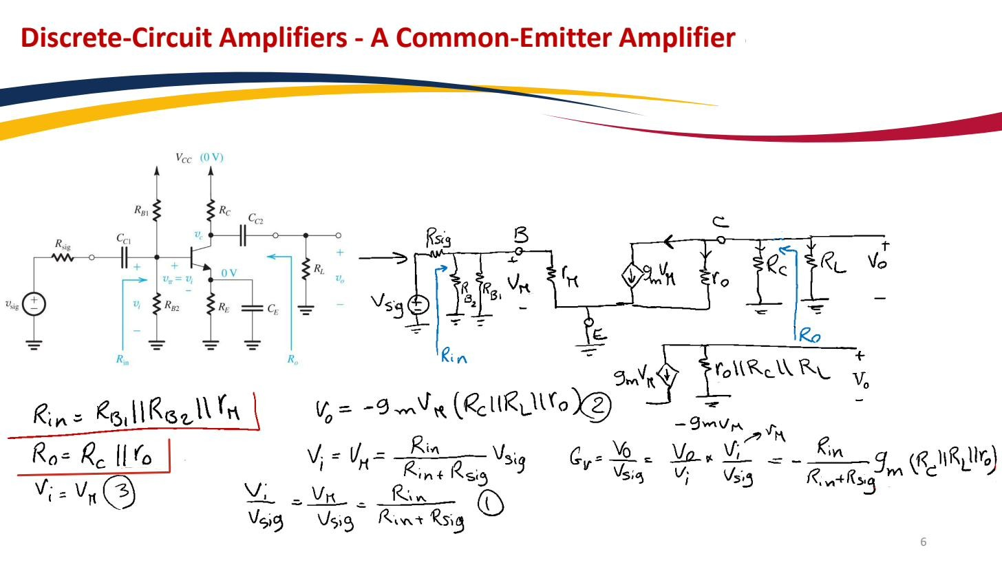 Discrete-circuit common-emitter amplifier: voltage-divider bias for stability, input/output coupling capacitors and , emitter bypass capacitor to short for AC while leaving it for DC.
Small-signal input and output resistance
With the bypass and coupling capacitors treated as AC shorts, the bias divider appears in parallel with the transistor’s [[BJT input resistance|]], and the output sees in parallel with the device :
 Coupling caps pass the signal and block DC; shorts for AC. The small-signal model gives and .
Common-base variant
The discrete Common-base amplifier uses the same four-resistor bias but the input is coupled into the emitter and the base is held at AC ground by a bypass capacitor. There is no emitter bypass capacitor: the emitter is the signal node, so it must not be shorted to AC ground.
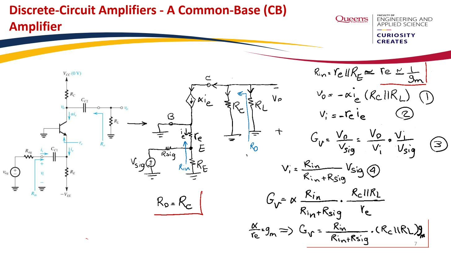 Discrete-circuit common-base amplifier: signal coupled into the emitter, base held at AC ground via a bypass capacitor.
Frequency response
These three capacitors also create the low-frequency rolloff. Each capacitor, with the resistance it sees, sets a low-frequency corner (); below that corner it stops being a good short/pass and the gain falls. The dominant low-frequency corner is usually the emitter bypass , because the resistance it sees (, often only tens of ohms) is the smallest of the three, which makes its corner the highest, so it is the last to “kick in” as frequency rises and therefore dominates the low end. At the high end the response is limited by the BJT’s internal and , the latter magnified by the Miller effect. That is why a CE stage has lower bandwidth than a CB stage built around the same transistor. See Amplifier frequency response.