A pnp transistor is the polarity-complement of the NPN transistor: a p-type emitter, a thin n-type base, and a p-type collector. Same physical principle, every voltage and current direction reversed, the way a p-channel device mirrors an n-channel MOSFET.
In an npn the emitter injects electrons into the base; in a pnp the emitter injects holes from the p-type emitter into the n-type base. Most of those holes diffuse across the thin base and are swept to the collector by the reverse-biased collector–base junction, exactly as in the npn case but with holes instead of electrons.
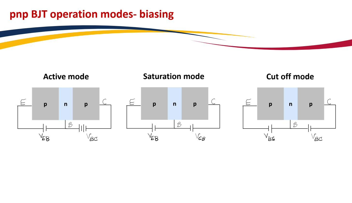 pnp BJT operation modes: the same three regions (active, saturation, cut-off) as the npn, but with inverted polarities.
Active-mode biasing
For a pnp in active mode the EBJ must be forward-biased and the CBJ reverse-biased, which (because the doping is reversed) means the opposite terminal polarities to an npn:
- The emitter–base junction is forward-biased with the emitter positive: (mind the order, it is , not ).
- The collector–base junction is reverse-biased with such that the collector is negative relative to the base.
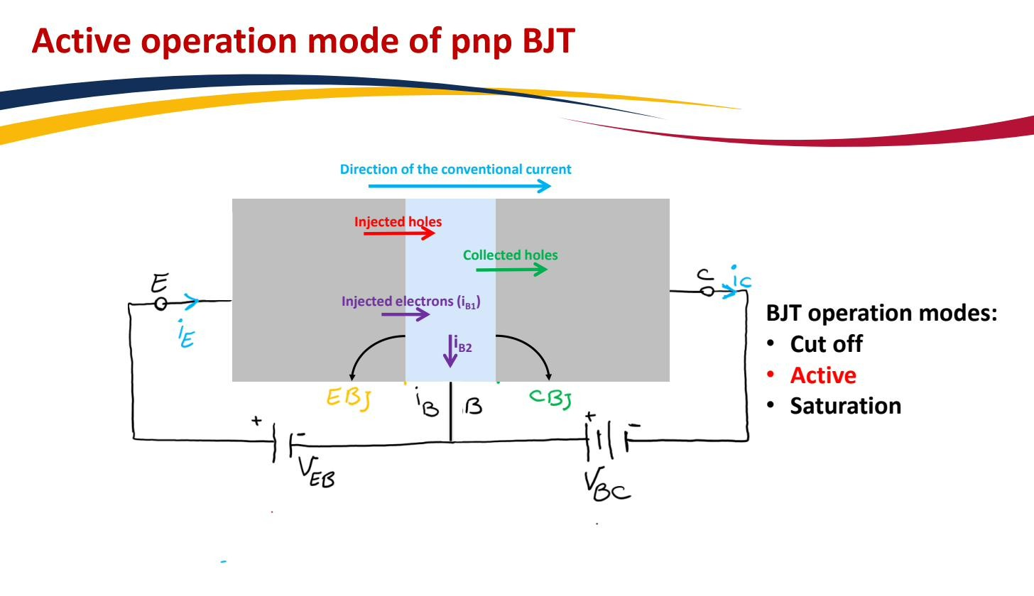 Active operation of the pnp: holes injected from the p-type emitter into the n-type base, most crossing to the collector. The direction of conventional current is opposite to the npn case.
Because the moving carriers are holes flowing emitter → base → collector, conventional collector current flows out of the collector terminal (and into the emitter), the reverse of the npn. The current-gain relations are unchanged in form:
with the Common-emitter current gain and the Common-base current gain. The same KCL holds at the device because there are still only three terminals.
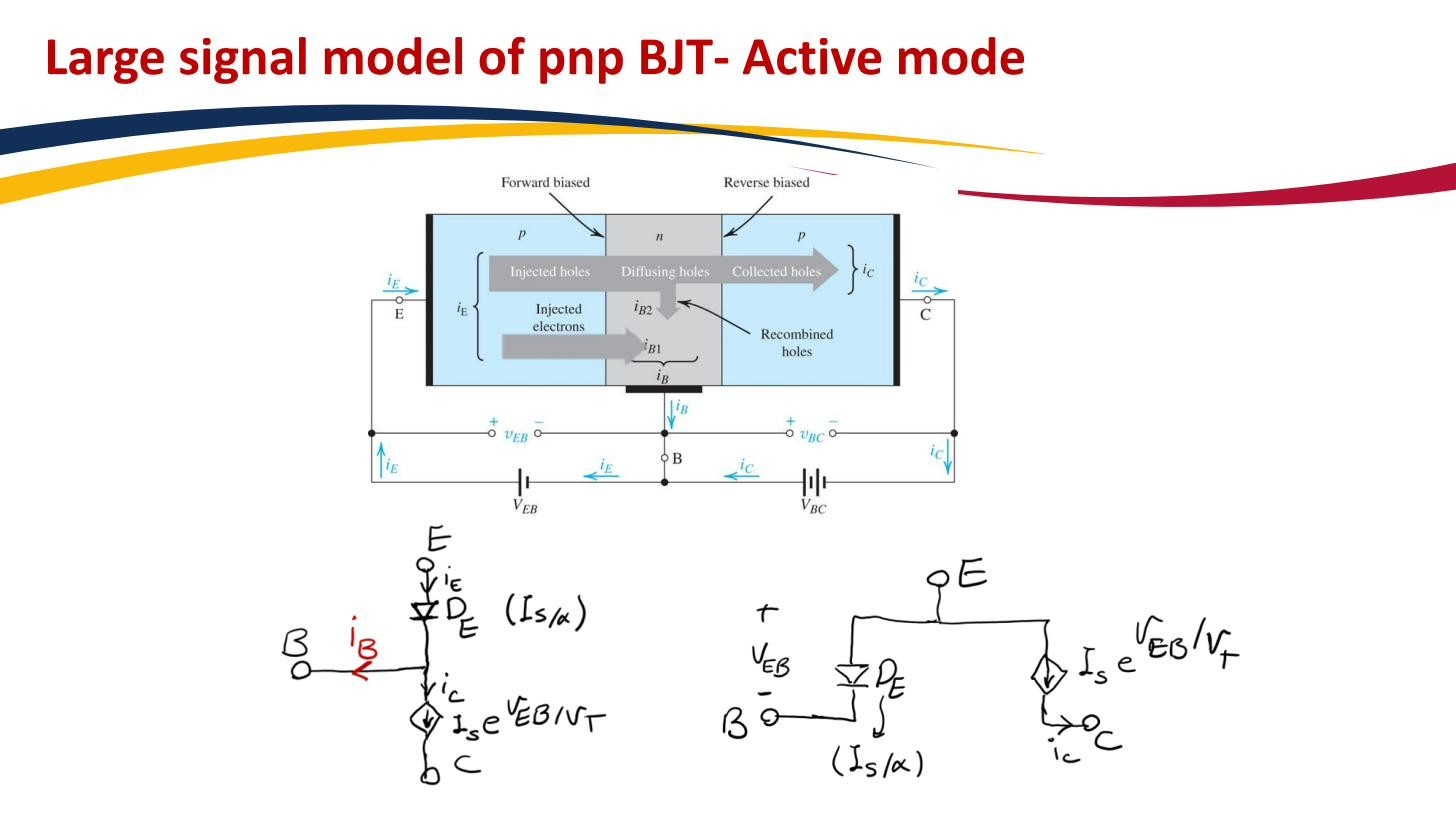 Large-signal model of the pnp in active mode: same structure as the npn BJT large-signal model but with the EBJ diode polarity reversed and the collector current source pointing the other way.
The pnp’s circuit symbol has the emitter arrow pointing in (emitter → base), the direction of conventional emitter current in active mode, opposite the npn’s outward-pointing arrow. A worked dual-supply pnp bias calculation is in BJT DC analysis. pnp devices are slower than npn devices of the same size because holes have lower mobility than electrons, so npn is the default; pnp is used where the circuit needs the complementary polarity (current sources to a positive rail, push-pull output stages, level shifting).