Small-signal analysis handles a non-linear device carrying a DC bias and a small time-varying signal at the same time. Find the DC operating point with the full non-linear model, then linearise the device about that point and treat the small signal with ordinary linear circuit analysis. Every amplifier here (diode, MOSFET, BJT) is analysed this way, with the same three steps and only the device’s small-signal element changing.
Why split DC and AC at all
The diode and transistor are non-linear: doubling the input does not double the output. You can’t just solve the circuit, because superposition doesn’t hold for non-linear elements. The escape is that the signal is small. Around a fixed bias point the device’s – curve is approximately a straight line (Linearisation around an operating point), and a straight line is a linear element. So you do the non-linear work once, at DC, to find where on the curve you sit; the small wiggle around that point sees only the local tangent, which is linear, and linear circuits obey superposition.
The three-step procedure
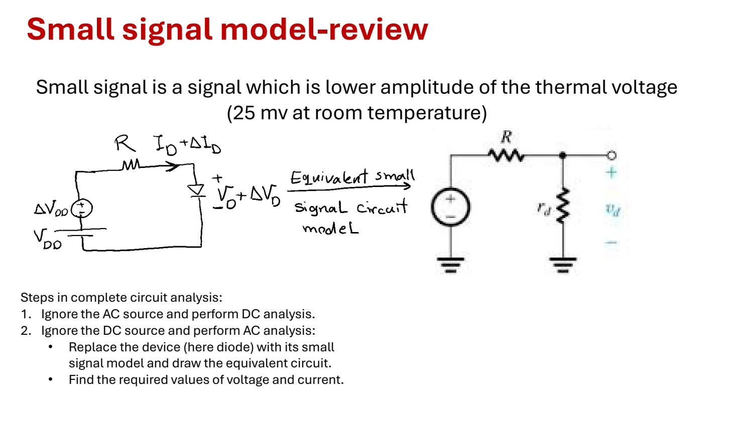
Step 1 — DC analysis. Set all AC (signal) sources to zero. Find the Operating point of every device using its large-signal model: the Constant-voltage-drop model or Exponential diode model for a diode, the square-law model for a MOSFET. This gives the DC currents and voltages (, , , …) the device sits at with no signal.
Step 2 — AC small-signal analysis. Set all DC sources to zero: replace DC voltage sources with short circuits and DC current sources with open circuits. Replace each device with its Small-signal model (for a diode, the resistance from Step 1). Solve the resulting linear circuit for the small-signal output.
Setting DC voltage sources to shorts and DC current sources to opens is the Superposition principle applied to the linearised circuit: a fixed source contributes nothing to the change in a quantity. A voltage source that doesn’t change is, to a varying signal, indistinguishable from a short (zero AC voltage across it); a current source that doesn’t change looks like an open (zero AC current through it).
Step 3 — Combine. The total voltage or current at any node is the DC value from Step 1 plus the AC value from Step 2. The DC sets where the device operates; the AC is the signal swinging about that point.
 Step 1 DC (operating point); Step 2 AC (device → small-signal model); Step 3 total = DC + AC.
The same procedure everywhere
The method doesn’t change from device to device. Only the small-signal element swapped in at Step 2 differs: for a diode (see Diode small-signal resistance), the , pair for a MOSFET, the , , set for a BJT. Once you can do it for a diode you can do it for any amplifier, which is why the diode example is taught first. Linearisation around an operating point covers why the tangent approximation is legitimate and what limits its validity.