Doping is the deliberate introduction of a small, controlled amount of impurity atoms into a pure Semiconductor to set its conductivity and decide which sign of carrier dominates. It turns nearly-inert intrinsic silicon into a usable device material, and it’s the reason diodes and transistors exist at all.
The one-electron trick
Silicon is in group IV: four valence electrons per atom, all used up in covalent bonds with four neighbours. Doping substitutes in an atom with one electron too many or one too few:
- Group V impurity (phosphorus, arsenic): five valence electrons. Four go into bonds with silicon neighbours; the fifth isn’t needed for bonding and is only loosely held, so at room temperature it breaks free and becomes a mobile electron. The impurity is a donor, and the result is n-type silicon, where negative electrons are the majority carrier.
- Group III impurity (boron, aluminium): three valence electrons. It can only complete three of the four surrounding bonds; the fourth bond is short an electron. It readily accepts an electron from a neighbouring silicon bond, and the vacated bond becomes a mobile hole. The impurity is an acceptor, and the result is p-type silicon, where positive holes are the majority carrier.
Only a tiny dose is needed. Typical dopant concentrations of – are minute next to silicon’s atoms (roughly one impurity per million-to-billion silicon atoms), yet they swamp the intrinsic carrier concentration of by many orders of magnitude and take over the conductivity completely.
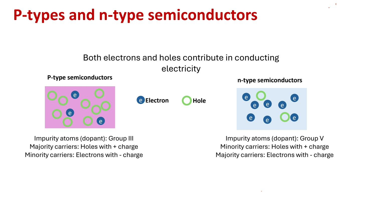 p-type and n-type side by side. Together they form the pn junction, the building block of every semiconductor device.
Doping does not break the mass-action law
The subtlety: doping changes the balance of carriers enormously, but the product stays pinned at by the Mass-action law. Add donors to make (donor concentration), and the hole population is forced down to . Not because holes were removed, but because the higher electron population speeds up recombination until is back to . So doping trades one carrier type up at the exact expense of the other:
Why it is the foundation of everything
A controllable, locally-defined carrier population is what makes semiconductor devices possible. Dope one region p-type and the adjacent region n-type in the same crystal and you get a PN junction, the asymmetric one-way conductor underneath every Diode and Transistor. Patterning n and p regions precisely on a wafer is the entire basis of integrated-circuit manufacturing.