A PMOS transistor (P-channel MOSFET) is the opposite of an NMOS transistor: it conducts when its gate is below its source by enough, and turns off when its gate rises toward the source. The exact turn-on condition is
where is the PMOS threshold voltage, conventionally written as a negative number (e.g. ); is its magnitude. With the source tied to and the gate driven to , , which is well above , so the PMOS conducts strongly. With , and the device is off.
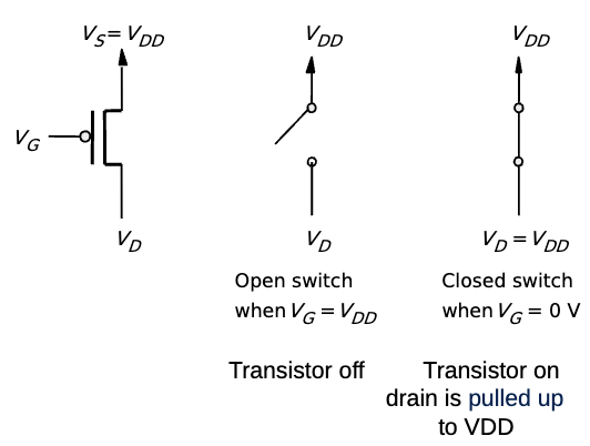
That’s why PMOS sits in the pull-up network of a CMOS gate. The little circle (“bubble”) on a PMOS gate symbol is shorthand for “active low” — turn this on by driving its input low.
Why PMOS is slower than NMOS
The carriers in a PMOS are holes. Hole mobility in silicon is roughly 2–3× lower than electron mobility, so for the same geometry and overdrive, a PMOS produces 2–3× less drive current than an NMOS. That means slower charging of a load capacitance, i.e. slower rising edges. CMOS designers usually size PMOS transistors physically wider than the matching NMOS (a typical ratio is 2:1 W/L) to compensate and balance rise and fall times at the output.
PMOS is one of the two transistor types in every static CMOS gate. Pass-transistor logic, dynamic logic, and transmission gates use them in different ways.
Physical structure and analog operation (Electronics I)
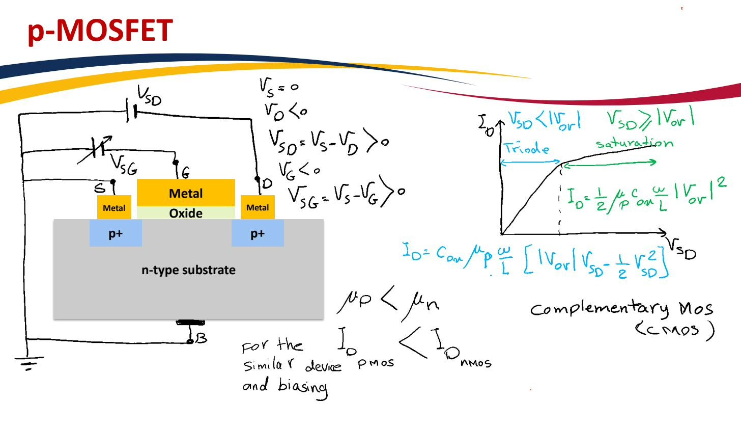
A p-MOSFET is the complement of the n-MOSFET: an n-type substrate with heavily-doped p+ source and drain, and a channel of mobile holes (not electrons) when on. Its threshold is negative and it conducts when . Because hole mobility in silicon is roughly 2–3× lower than electron mobility, a p-MOSFET of the same and carries only about a third to a half the current of an n-MOSFET, which is why CMOS layouts draw p-MOSFETs 2–3× wider to balance drive. In analog use it has the same three MOSFET regions of operation as the n-MOSFET, all with inverted polarities (, , negative).
 p-MOSFET: p+ source/drain in an n-substrate; hole channel, inverted polarities.