The depletion region width is the total thickness of the Depletion region of a PN junction, split into a part on the n-side and a part on the p-side. Doping concentrations and the bias set its value.
where:
- = depletion depth into the n-side, = depletion depth into the p-side.
- = permittivity of the semiconductor (for silicon ).
- = electron charge, .
- , = acceptor and donor doping concentrations.
- = the Built-in voltage (in equilibrium; under bias, replace it with the total junction potential, see below).
Where it comes from (Poisson’s equation)
Poisson’s equation relates the electric field to charge density: . Inside the depletion region the only charge is the fixed dopant ions, so on the n-side and on the p-side . Overall charge neutrality of the exposed charge requires the positive charge on the n-side to balance the negative charge on the p-side:
Integrating Poisson’s equation once gives the (triangular) field profile, peaking at the junction; integrating again and evaluating the total potential drop across both sides sets that drop equal to . Solving for the total width produces the boxed expression above. The combination falls out of eliminating and with the neutrality condition.
Two consequences worth remembering
1. The lightly-doped side gets the wider depletion. From , the side with more doping has the smaller depletion depth, so the depletion mostly extends into the lightly-doped side. A region needs a certain amount of fixed charge exposed to support the field; if the doping density is low, you have to deplete a wider slab to expose that much charge. So in a junction (heavily doped p, lightly doped n) almost all of lies on the n-side.
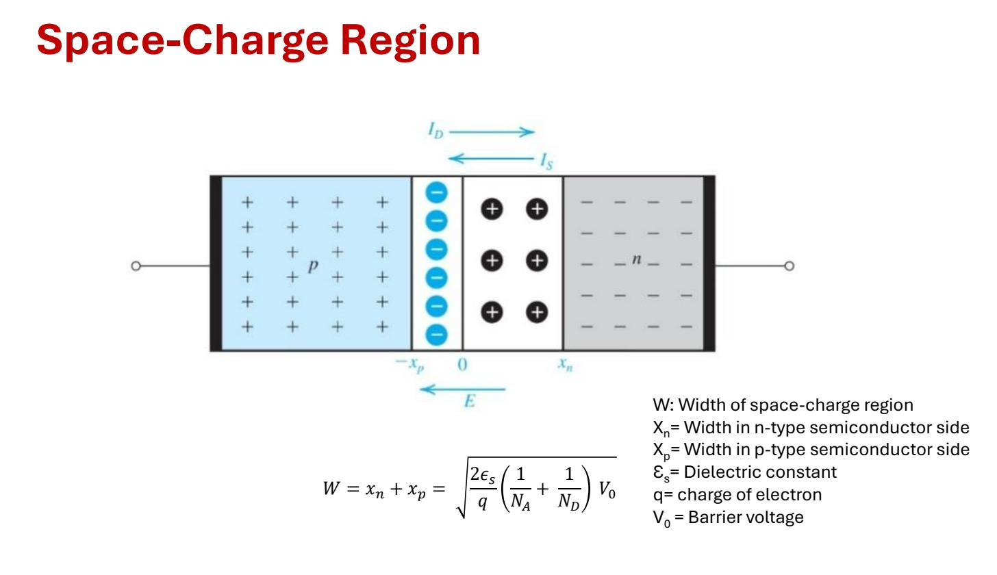 Width splits into and ; the heavier-doped side has the narrower depletion.
2. Bias changes the width. An applied voltage changes the total potential the depletion region must support. Replace in the formula with the net junction potential:
- Reverse bias (applied adds to the barrier): total potential , so increases, the region widens.
- Forward bias (applied opposes the barrier): total potential , so decreases, the region narrows.
This voltage-controllable width is why a reverse-biased junction behaves like a voltage-variable capacitor (a varactor), and it’s central to how field-effect and bipolar transistors modulate current.